Every year, the UIUC chapter of ACM has an student-run conference called Reflections|Projections . One (rather excellent) speaker at the 2013 conference was the well-spoken (and wickedly-smart) Todd Fernandez , who spoke about the state of the semiconductor integrated circuit industry. As a nice bonus for those brave souls who asked, or answered, a question during his talk, he was giving out junked silicon wafers. Not being much of a brave soul myself, but realizing that the wafer would make for an awesome sample in our now-functioning Scanning Electron Microscope (SEM), I answered a question about Moore’s Law and scored a wafer.
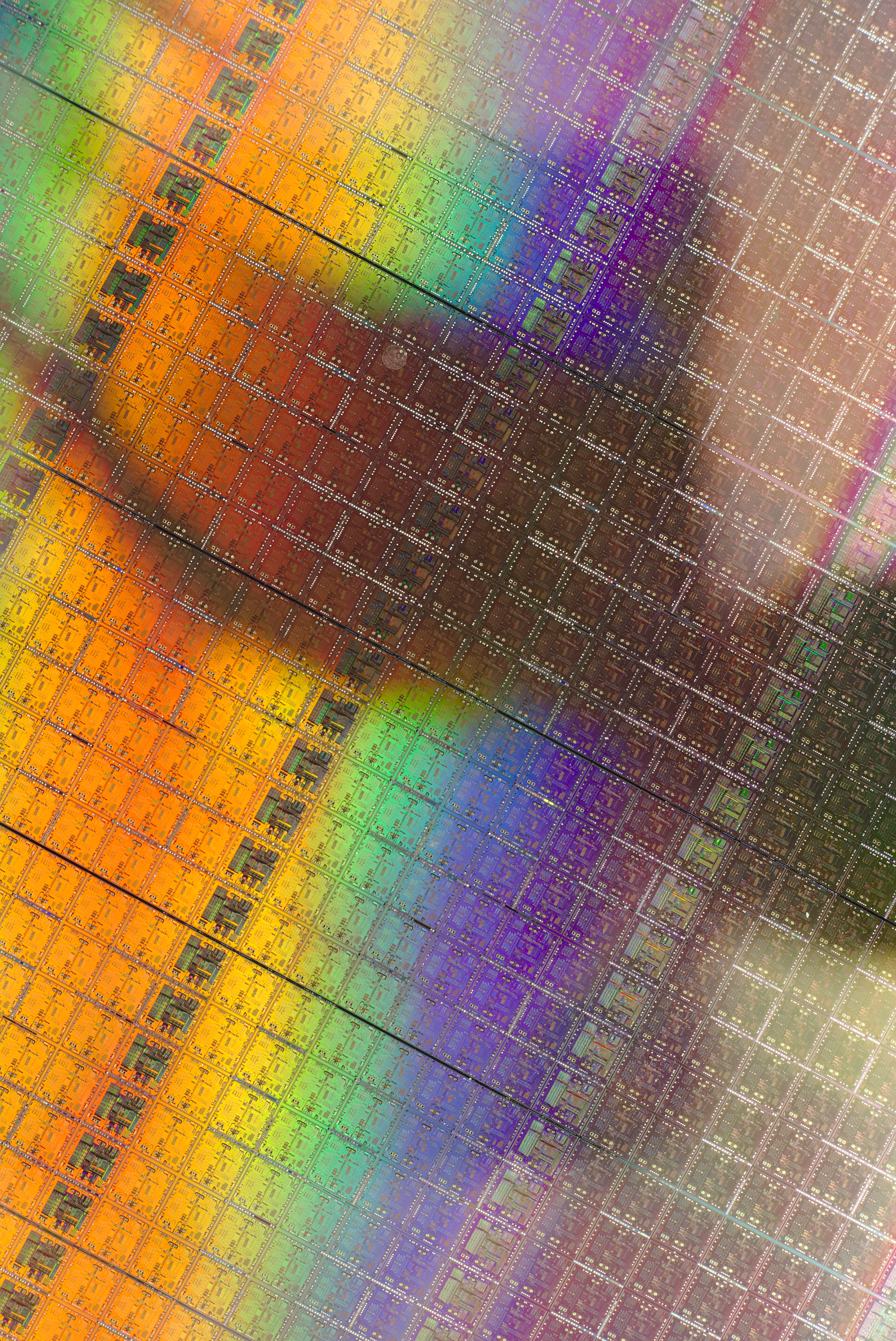
Saving you a trip to Wikipedia: the wafers are slices of an impressively large and pure single crystal of silicon (known as a boule) on which semiconductor devices (such as transistors) are fabricated. These devices are usually incredibly tiny and incredibly numerous.
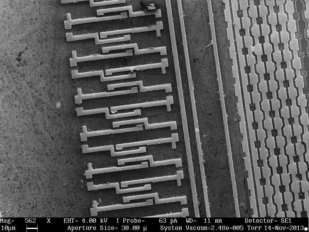
What happens after that is that the SEM rasters a beam of electrons across the surface of the wafer sample and, in this particular case, utilizes its ability to detect secondary electrons kicked off the wafer by the beam. Because the surface is the important part and because the SEM’s resolution is so amazing, before we mounted the sample, we had to sterilize it in an acetone bath suspended in the space’s ultrasonic cleaner.
Now the cool part. Because, if you look at the picture below, you can easily see leads on the wafer that are 4 microns in width (and resolve gaps between the leads that are 2 microns wide). For reference’s sake, the diameter of a human hair is given as 100 microns on average. And that is awesome.

Many thanks to the exceptional Ryan Pierce, who helped me with this every step of the way.
-Jerry Lebedowych